Reciprocity failure in color film

While working on my slide collection digitization project, I came across some classic examples of color film reciprocity failure.  This is not a problem with modern digital photography, but something one should be aware about, otherwise it will surprise you when it crops up..

For starters, let’s consider the concept of reciprocity. Reciprocity refers to the simplification that the response of silver halide is a function of the total exposure. As a result, you should be able to achieve the same density of silver grains by exposing to a fixed total amount of light.  This fixed amount  is equal to the exposure time multiplied by the light intensity.  The idea is that the same density is achieved, say, intensity I in one second and with half the intensity or I/2 in two seconds.  Film does not strictly respond in this way.  At extremely low light levels this is not strictly true – hence what is known as reciprocity failure.  At low levels of
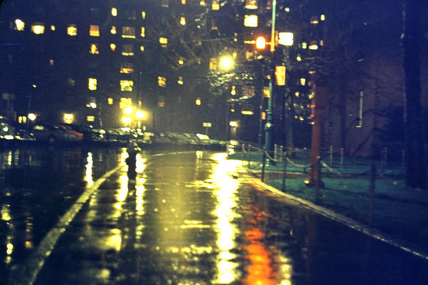
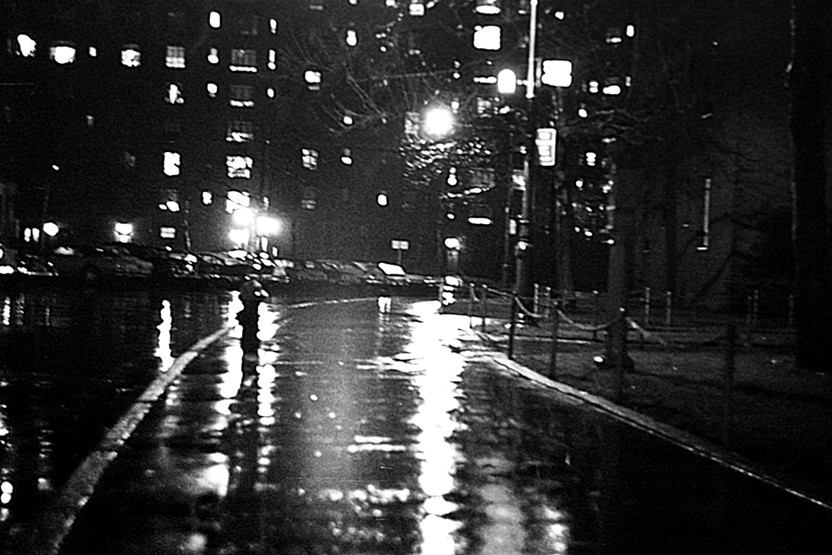
Figure 2 - Uncorrected digitized Ektachrome image of a wet street at night in NYC, illustrating reciprocity failure. (c) DE Wolf 2013.

Figure 1 – Uncorrected digitized Ektachrome image of a wet street at night in NYC, illustrating reciprocity failure. (c) DE Wolf 2013.

light the film responds much more slowly so you need a longer exposure to get the same density on your negative.  For color films things become more problematic as each of the three color layers respond differently to low light level.  In general, with slide films green is more responsive than yellow; so the image slips into a greenish tinge.

This can easily be seen in Figure 1, a digitization of an Ektachrome transparency, taken around 1970, of a New York City Street on a rainy night.  The image has clearly, shifted towards the green.  You’ve got to decide whether or not you find this aesthetically pleasing.  Of course, once you’ve got the slide digitized it is a simple matter to adjust the color back to normal, which I have done in Figure 3.  So you can decided which image you like better: uncorrected Figure 1 or corrected Figure 2.

Figure 2 - Color-corrected version of Figure 1.  (c) DE Wolf 2013.

Figure 2 – Color-corrected version of Figure 1. (c) DE Wolf 2013.

I showed this image to several colleagues, and it was unanimously decided that, in fact, the image looked better as a black and white.  This is presented below as Figure 3, and speaks to the power of black and white photography to create mood.

Figure 3 - Night scene of NYC in the rain, c 1970," (c) DE Wolf 2013.

Figure 3 – Night scene of NYC in the rain, c 1970,” (c) DE Wolf 2013.


Building a digital camera sensor from a charge coupled device

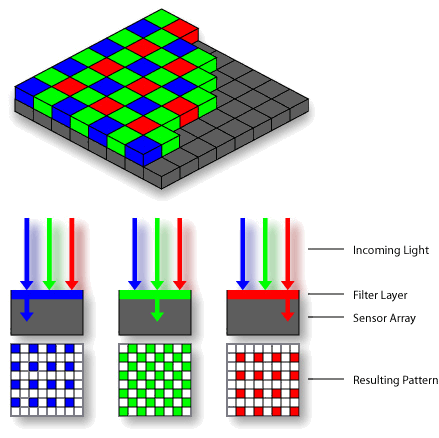
Figure 1 - Schematic of Bayer filter overlain on a CCD (top) also showing how rede, blue, and green light is separated by the filter.  From the Wikicommons and in the public domain.

Figure 1 – Schematic of Bayer filter overlain on a CCD (top) also showing how rede, blue, and green light is separated by the filter. From the Wikicommons and in the public domain.

Now that we understand how a charge coupled device or CCD works and how it reads out, we are in a position to consider how exactly one goes about making a color digital camera sensor out of one.The first question is how does one make an intrinsically black and white sensitive sensor sensitive to color.  If you followed our discussion about autochromes and additive color, the answer is obvious.  You overlay the pixels with some kind of set of red, green, and blue filters.  Because everything needs to be electronically addressable and translatable from imaging device to display, say a computer screen, it’s better not to use a random distribution of filters, like in an autochrome, but rather an ordered one.  Figure 1 shows schematically such a filter system, referred to as a Bayer filter.

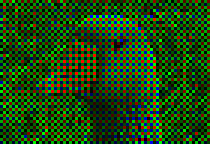
Figure 2 - Image acquired with a CCD chip through a Bayer filter.  From the Wikicommons and in the public domain.

Figure 2 – Image acquired with a CCD chip through a Bayer filter. From the Wikicommons and in the public domain.

Notice that we have twice as many green filters as we do red or blue filters.  The reason for this is that the human eye as twice as many green sensitive cells as it does red or blue sensitive ones.  Figure 2 shows an example of an image, where we have focussed in very closely so that we can see the individual filters of the Bayer filter.  You can do the same thing at home with  a digital TV or computer screen and a magnifying glass.  So far so good, but there’s a second very important question to consider – the question of how to make the sensor as sensitive as possible.  Even though the intrinsic quantum efficiency of a CCD can be remarkably high (as high as almost one electron per photon) several factors conspire against us.  There is dead space between pixels and off angle light isn’t going to make it to the photosensitive region.

If you look at Figure 3 you see a schematic of a cross section of a pixel that illustrates several aspects of camera sensor design.  Let’s walk through this.

  1.  is the incoming light.
  2.  is a lenslet that collects light to the pixel.  It can be shaped so that even light over dead zones makes it to the sensor pixel.
  3. is the Bayer filter element.
  4. is the transparent voltage gate.
  5. is the silicon dioxide insulator.
  6. is the n-doped silica layer
  7. is the p/n silica layer
  8. is the p-doped silica layer.
Figure 3 - Cross section of a pixel on a color digital camera CCD sensor.  From the Wikicommons and in the public domain.

Figure 3 – Cross section of a pixel on a color digital camera CCD sensor. From the Wikicommons and in the public domain.

The lenslets are very important elements.  Without them the device can become quite insensitive.  This is especially true as we push greedily for more and more pixels.  If you have a certain amount of light striking a pixel and then cut the pixel size in half, so that you have four pixels, where previously there was one, then each pixel gets only a quarter as much light.  The well depth similarly goes down.  So the bottom line is that you want as much signal as possible.  Signal compared to what?  Yes you guessed it.  Signal compared to noise!

More Secrets of Charge Coupled Devices

CCD_charge_transfer_animation

Figure 1 – Charge transfer in a CCD array. By Michael Schmid from the Wikicommons and under creative commons license.

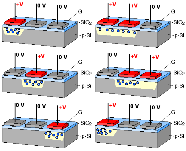
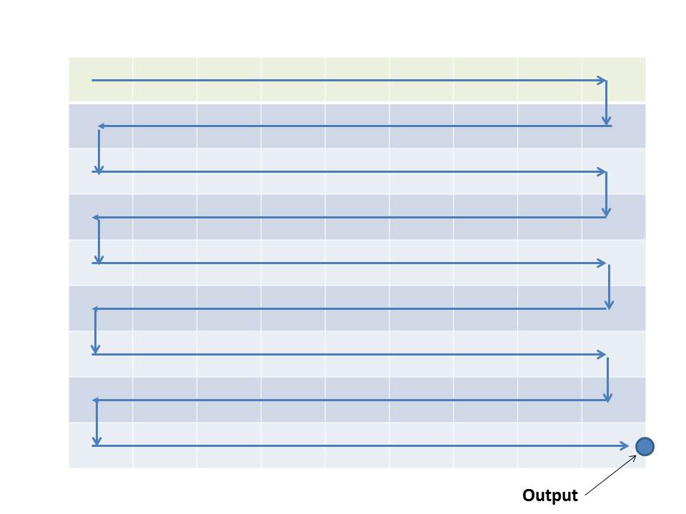
The real secret of a charge coupled device is how it uses programmed voltages to shift the stored charge between pixels.  This is illustrated schematically in Figure 1.  Once the exposure is complete.  The device systematically shifts the charge from pixel to pixel until it reaches the readout point.  This is accomplished as shown in the animation by taking a pixels voltage to zero which allows it to transfer to the adjacent pixel held at a voltage V. The process, illustrated in Figure 2 is not unlike a “bucket brigade.”

Figure 2 - The march of the electrons in a CCD sensor. (c) DE Wolf 2013

Figure 2 – The march of the electrons in a CCD sensor. (c) DE Wolf 2013

By the way, I think that you can see the advantage of using a shutter on a CCD camera.  It protects the sensor from light while it is in the process of reading out.

At the output the accumulated charge acts as a voltage.  A device known as a analogue to digital converter (A/D) converts this voltage to a digital signal.  Significantly the signal is analogue up until this point, when it becomes digitized.

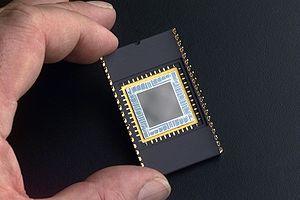
ChargeCoupled Array

Figure 3 – A CCD sensorarray. From NASA via the Wikicommons and in the public domain.

There’s a lot to talk about regarding CCDs.  However, let’s focus for now on two points, just to give a flavor.

  • As charge is transferred between pixels there’s a little slop over, just like spilling water in a bucket brigade.  As a result the readout process introduces a source of noise in the signal.  This means that the amount of charge transferred per pixel is variable because of the readout, in addition to all the other reasons that it can be variable.
  • The dynamic range of the device, that is the number of grey levels that it can be divided into is defined, not by the number of bits in the digitizer, but rather by the number of electrons.  We discussed many months ago the concept of  photon counting noise.  This is controlled by the number of electrons in the well, by the well depth.

You can also see that I am very focused on sources of noises.  This is what it’s all about.  If you want to know how sensitive of CCD is, or if you want to discuss proper exposure, or dynamic range, or ISO you’ve got to worry about what physicists and engineers call the signal-to-noise ratio.

But for now, we are getting ahead of ourselves.  And I’d like finally to show you a typical CCD sensor array, which is shown in Figure 3.


Secrets of Charge Coupled Devices (CCD)

Figure 1 - Schematic of the structure of a pixel element of a CCD array (c) DE Wolf 2013

Figure 1 – Schematic of the structure of a pixel element of a CCD array (c) DE Wolf 2013

In our last technical blog we discussed how semiconductor junctions can be used to create electrical signal.  This is a good start, and you can certainly imagine that if you made a two dimensional array of such photodiodes you would have an imaging devices.  There is one problem however.  The device that we described pumps out electricity at some rate.  While this rate can be adjusted, it gets hard to integrate signal for large amounts of time like we do with photographic film.  For this purpose the charge coupled device, the CCD, comes to our rescue.

There are a lot of fascinating and important points to consider about CCDs.  The first is how do they store your image until you have achieved sufficient exposure to read it out.  Take a look at Figure 1, which shows schematically the structure of a single pixel element of a CCD array.on.   First of all, notice that we have a gate, basically a metal electrode.  For starters it is held at a positive voltage.  Next we have a layer of silicon dioxide.  Yes sand!  And that’s an insulator that does not carry electrons.  It acts like a barrier that keeps the electrons away from the gate.  Then we have a thin layer (called an epitaxal layer)  of n-type silicon.  This is the photosensitive region, where electrons are easily stripped off by light.  The epitaxal layer sits on a layer of p-type silicon.  A negative voltage is applied to the back side of the p-type silcon layer.

What about the photoelectrons?  They can’t go to the gate.  They won’t go to the negative electrode on the back side.  So they start to fill up the holes in the p-type silcon layer below the gate.  The longer the device is exposed to light the more electrons are created and bound up by holes until there are no more holes available.  You can think of the holes as forming a well that collects electrons, and then the maximum number of electrons that the well can hold is the well capacity.

We seem to have just what the doctor order.  It is a device which stores charge proportionally to the light exposure. as a function of exposure.  It is effectively an electronic film.  You can certainly see how you can build up an array of these pixel.  So really the big question that remains is how to read it out.  That is the subject of our next technical blog.


Semiconductor light detectors

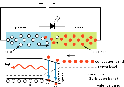
Figure 1 - schematic of the p-n junction of an LED.  Top shows distribution of electrons and holes in the two regions. Bottom shows the conductance and valence bands. From the Wikicommons by S-kei and in the public domain under creative common license.

Figure 1 – schematic of the p-n junction of an LED. Top shows distribution of electrons and holes in the two regions. Bottom shows the conductance and valence bands. From the Wikicommons by S-kei and in the public domain under creative common license.

We have previously discussed how a p-n junction can be used to produce a light emitting diode (LED) and how an array of LEDs can be used to create a digital display.  I redisplay Figure 1 from that blog to remind you.  So lets recall a few critical points.  First, the n-type semiconductor is rich in electrons.  Second, the p-type semiconductor is deficient in electrons, that is is rich in holes.  Second the application of a voltage across the diode (p side positive, n side negative) causes a current to flow and drives electrons from the n-type semiconductor to the junction, where they combine with holes; thus falling out of the conduction band into the valence band.  When they do this, they emit light.  Hence, we have a light emitting diode.

Now the whole process can, in fact, be reversed.  Physicists have a really cool expression.  They say that “the system is invariant under reversal of time.”  Whoa! Time reversal. Shades of H. G. Wells.  Actually this whole question of time reversal in physics is rather fun.  In our everyday world time is an arrow.  It moves from the past to the present and then on to the future – in inexorably.   But the equations of physics they don’t care they can go either way.

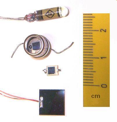
Figure 2 - Examples of discrete photodiode light detectors.  From the Wikicommons and in the public domain under GNU licsense

Figure 2 – Examples of discrete photodiode light detectors. From the Wikicommons and in the public domain under GNU licsense

And for our little p-n junction this means that if we can apply a current (aka electricity) and create light we can apply light and get electricity.  So if you have a p-n junction and shine light on it (at the correct wavelength), electrons get lifted from the valence band to the conductance band.  What happens next depends on whether you have a battery hooked up to it.  If you don’t then the electrons build up at the junction creating an electric field or a voltage.  The size of the voltage depends upon the amount of light.  This is the so-called photovoltaic mode.  On the other hand if you attach a battery in the opposite to that shown in Figure 1 (meaning that the plus side is attached to the n-type material and the minus side to the p-type material, referred to as reverse bias) then the as electrons rise to the conductance band they are swept to the positive battery terminal, a current is created.

The reason that the battery needs to be set up reverse bias or backwards to that shown in Figure 1 has to do with our desire to run the system in reverse time.  If running electrons one way causes light, we expect that light will cause the electrons to run the other way.

So we can use a p-n junction to create light, a light emitting diode.  And we can use a p-n junction to create either a voltage or a current.  The latter means that we can use a p-n junction to measure light.  Some example of discrete (stand alone) photodiodes are shown in Figure 2. These devices are at the heart (eyes?) of how many light meters on cameras work.  And we are one step further to understanding how a digital camera’s detector array works.


P-n junctions and the heart of the LED display

Figure 1 - schematic of the p-n junction of an LED.  Top shows distribution of electrons and holes in the two regions. Bottom shows the conductance and valence bands. From the Wikicommons by S-kei and in the public domain under creative common license.

Figure 1 – schematic of the p-n junction of an LED. Top shows distribution of electrons and holes in the two regions. Bottom shows the conductance and valence bands. From the Wikicommons by S-kei and in the public domain under creative common license.

We now have the background information about semiconductors that we need to start to talk about digital photography – about digital array displays and digital sensor arrays.  Let’s start with a discussion of LED (light emitting diode) displays.  If you sigh at this point and try to escape to elsewhere on the web, chances are that an LED display will still be staring you in the face.  If you instead try to escape by watching television, the chances are still very high that an LED display is staring you in the face.  So under the assumption that it’s worth knowing as much about your computer as it knows about you, let’s proceed.

In my last technical blog, I discussed p and n type semiconductors.  In and of themselves, they’re not too exciting.  However, the fun begins when we start to combine them.  Suppose we put a p type semiconductor right up against an n type semiconductor.  This is what is called a p-n junction.  This is also called a diode and is shown graphically in Figure 1, where we’ve even allowed for a small transition region.  The p region is shown in blue and the n region in green.  You’ll note that we’ve connected this to a battery.  The plus terminal to the p side and the negative terminal to the n side, as one might expect.  Once the battery is connected, the electrons start to flow towards the plus terminal (remember that opposites attract).  Remember also that electrons can flow.  Holes really only appear to flow because the electrons are flowing.  So there is a current in the semiconductor, with electrons flowing from the n region into the p region and on to the plus terminal of the battery.  Of course, electrons exit the negative terminal of the battery and enter the n side of the diode.  If you hooked the battery up backwards there would be no current.  A diode is unidirectional.

As an aside, in the center we see the symbol for a diode, with its big honking arrow showing the direction that current flows.  This is because back in the eighteenth century no less than Benjamin Franklin made the unlucky guess that the charge carrier was not the negative but the positive charge, and this view is perpetrated by convention in circuit theory today, even though everyone knows that it is wrong.

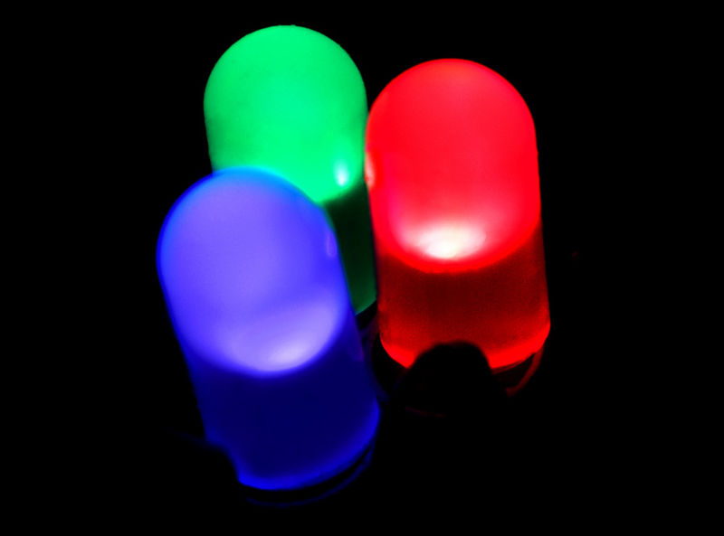
Figure 2 - Large size red, green, and blure LEDs the fundamental components of an LED display.   From the Wikicommons by PiccoloNamek  and in the public domain under creative common license.

Figure 2 – Large size red, green, and blure LEDs the fundamental components of an LED display. From the Wikicommons by PiccoloNamek and in the public domain under creative common license.

The key thing about the light emitting diode (LED) is that when the electrons enter the p region they recombine with and neutralize holes.  This represents as shown in the lower portion of the schematic a transition from the conductance band back to the valence band with the emission of light whose color depends on the transition energy.  Hence, electrical energy is converted to light at the junction.

In Figure 2, I show diodes of the three primary colors: red, green, and blue.  If you take a magnifying glass up to your LED display, you will see minute arrays of these red, green, and blue LEDs each of which is individually addressable, meaning the light intensity of each can be individually controlled so that whatever color you and intensity you desire is created by additive color.  That is basically, how an LED display works.

P and n type semiconductors – doping and stacking the odds in your favor

Figure 1 - Schematic of a semiconductor crystal at absolute zero where all of the electrons are bound up by holes.

Figure 1 – Schematic of a semiconductor crystal at absolute zero where all of the electrons are bound up by holes.  (c) DE Wolf 2013.

As we have seen, the fundamental silver halide chemistry of analogue photography depends upon the physics of semiconductors.  And yet, it was developed before anyone knew about semiconductors or even uttered the word.  Indeed, in those days they didn’t need to utter the word “analogue” in relation to photography, because there was no digital photography to contrast it with.  The same is true for watches.  In the “dinosaur ages,” when I was a lad, there were just watches not analogue watches and certainly not digital watches.  Indeed, the time is fast approaching when there may be no watches except during retro-fashion fads.

But, as I promised, semiconductors will explain a lot of the technical aspects of digital photography.  To get there we need to discuss one more aspect of semiconductor physics – qualitatively I promise.

At absolute zero the valence electrons have no excess kinetic energy and are all sitting in their valence bands.  This is shown in Figure 1.  All of the positively charged holes are paired up with negatively charged electrons – very boring.  Now as we heat up the semiconductor to room temperature, some of the thermal (heat) energy gets absorbed by the electrons and they can escape to the conduction band where they are free to move.

Figure 2 - Schematic of a semiconductor crystal at room temperature where some of the electrons have escaped the lattice and are in the conductance band.  There are functionally two types of charge carriers: the free electrons and the positive holes. (c) DE Wolf 2013.

Figure 2 – Schematic of a semiconductor crystal at room temperature where some of the electrons have escaped the lattice and are in the conductance band. There are functionally two types of charge carriers: the free electrons and the positive holes. (c) DE Wolf 2013.

Free to move means that if I attach a battery to two sides of the crystal current will flow.  Recognize, that as they flow in the current some electrons may recombine with holes.  But then new holes appear as new electrons escape and the net effect is that electrons move form the negative side of the battery to the positive side (remember that opposites attract).

But wait! Imagine that you are watching this process from  a distance.  Is it the electrons that are moving or is it the holes.  They both appear to be moving.  It’s like the sensation of being on a train and suddenly the platform appears to be moving.  Of course, we know that the electrons have escaped the crystal lattice, while the atoms (holes) have not.  But it does look like the holes are moving, and you can even calculate a speed for this motion.

The next question that we need to ask is whether there is a way of modifying the semiconductor crystal so that has more electrons or more holes?  Well, remember that whether a material is a conductor, a semiconductor, or an insulators depends on how tightly the valence electrons are bound to the positive atomic nuclei.  Remember also that the solid-state crystal acts as a unit not as a set of individual atoms.  The net-net of all of this is that if we add a small amount of a material that tends to donate electron the crystal will have more free electrons (in the conductance band).  If we add a small amount of a material that tends to bind up electrons (in the valence band) it will have more holes.  The materials added are called “doping agents.”  Semiconductors with excess negative charge (electrons) are called “n-type semiconductors.”  Semiconductors with excess positive charge (holes) are called p-type semiconductors.

The cool thing is that doping can be a very localized process, and as a result, you can build up some very complex semiconductors capable, for instance, of creating a computer and displaying your photographs on a light emitting diode display.  That will be the topic of our next technical blog.

How is the latent image developed, stopped, and fixed?

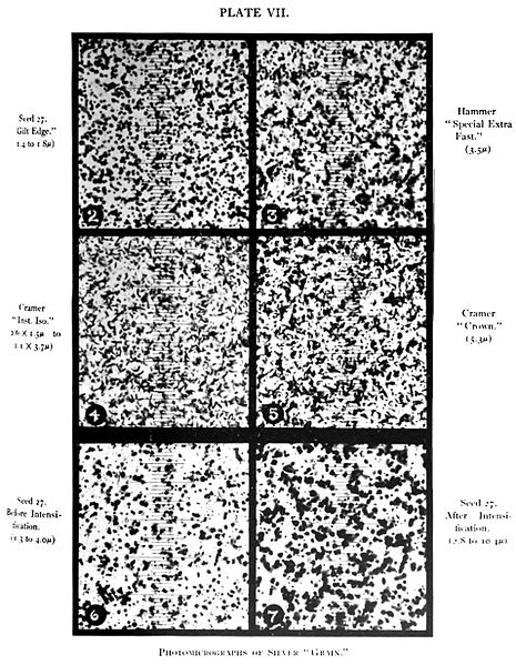
Figure 1 - Silver halide photographic grains, from the Wikicommons and in the public domain.  Originally from Plate VII from Robert James Wallace, "The Silver 'Grain' in Photography" by Robert James Wallace, The Astrophysical Journal, Vol. XX, No. 2, Sept. 1904, pp. 113–122, Chicago.

Figure 1 – Silver halide photographic grains, from the Wikicommons and in the public domain. Originally from Plate VII from Robert James Wallace, “The Silver ‘Grain’ in Photography” by Robert James Wallace, The Astrophysical Journal, Vol. XX, No. 2, Sept. 1904, pp. 113–122, Chicago.

Today, let’s continue with our discussion of the silver halide process.  In our previous blog, we discussed the latent image, how it was made, and how you cannot see it.  We discussed how a silver ion in the silver bromide, AgBr, grain, Ag+, gained an electron and became free silver, Ag.  This process of gaining electrons in chemistry is called “reduction.”  Now, there are lots of chemicals that can contribute electrons and, yes, you guessed it, they are called “reducing agents.”  In photography they’re also called “developers.”  Usually the developers used in photography are organic compounds, but that’s not a critical point.

Now the key to all of this is that a crystal of silver bromide will not be reduced to free silver unless it already has some free silver in it.  Remember the latent image?  The free silver kind of primes the pump for the reducing agent.  There are two fancy phrases used in chemistry for this pump priming process.  We say that the free silver catalyzes the production of free silver in those grains were it already exists.  Alternatively, we say that the free silver acts as a nucleation site for the production of more free silver.

In any event, the effect of all of this is that those grains which had free silver, that is are part of the latent image, undergo reduction to produce more free silver.  In contrast those which had no free silver are unaffected by the developer.

This is great! Right?  We now have lots of dense silver grains (see Figure 1) on the parts of the emulsion, which were exposed to light.  So can we turn on the lights now and see the image?  Absolutely, not.  The problem is that there is still lots of unexposed and, therefore, still light sensitive silver bromide in the emulsion.  So there are a few more steps in the development process.

First, you need to stop the action of the developer.  While this can be done by rinsing in water, when you are looking for good control of the process, it is more typical to use an acid stop bath that stops development in its tracks.  This makes a lot of sense, since, by definition, an acid provides lots of positively charged protons ready to steal away any remaining electrons.

Then the remaining silver bromide needs to be removed. This is generally done using sodium thiosulfate, otherwise known as hypo.  This solublizes the free silver bromide out of the emulsion by converting it to bromine and silver thiosulfate ions.  These can then be safely washed away, and if you do a good job with your washing, the image stays clean for a hundred years or more.

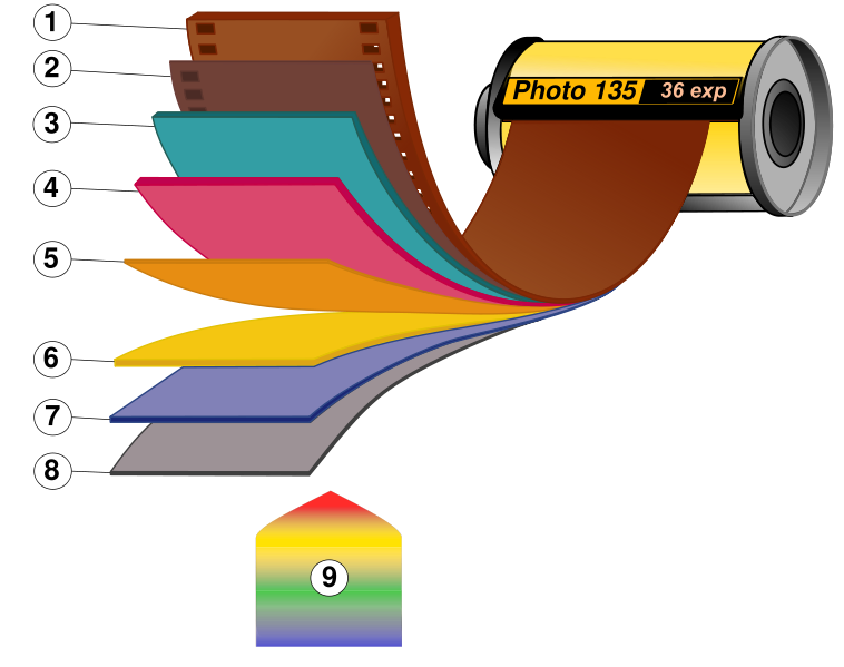
Figure 2 - a modern color photographis film showing the different layers. 1. Film base; 2. Subbing layer; 3. Red light sensitive layer; 4. Green light sensitive layer; 5. Yellow filter; 6. Blue light sensitive layer; 7. UV Filter; 8. Protective layer; 9. Visible light. From the Wikicommons, byVoytek S under creative commons liscense.

Figure 2 – a modern color photographis film showing the different layers. 1. Film base; 2. Subbing layer; 3. Red light sensitive layer; 4. Green light sensitive layer; 5. Yellow filter; 6. Blue light sensitive layer; 7. UV Filter; 8. Protective layer; 9. Visible light. From the Wikicommons, by Voytek S under creative commons liscense.

This is pretty much all that there is to it.  But let’s take a moment to reflect.  This brilliant concept was created and refined by hundred of chemists, physicists, and engineers over the course of more than a century.  The wonderful complexity is hidden in what seems very simple.  Therein lies the magic!  The gelatin, for instance, has to allow all the chemistry to occur, allow the removal of unreacted silver bromide, but then offer some reasonable level of mechanical stability for the silver grains for a hundred years or more – and we’re doing this with what? – egg whites and animal bones.  It’s really truly marvelous.  Figure 2 shows a modern color film with all its complex layering required to produce a subtractive color image as we have discussed previously.  And remember, at the root of all of this is the basic silver halide photgraphic process.

How is the latent image formed?

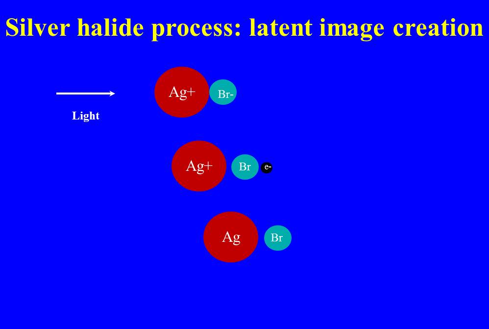
FIgure 1 - Schematic showing the creation of a latent image upon exposure to light in a silver bromide emulsion. (c) 2013 DE Wolf

FIgure 1 – Schematic showing the creation of a latent image upon exposure to light in a silver bromide emulsion. (c) 2013 DE Wolf

You will recall that photography was invented in 1838.  So the light sensitivity of silver salts, such as silver bromide, was recognized for a very long time.*  However, it was not until 1938 that a real theoretical-mechanistic explanation of this sensitivity began to be developed.+  We have already discussed the concept of valence and conduction bands in silver halides and how light can raise electrons between these two bands.  Recognize however, that when the electron is elevated in energy to the conduction band it leaves behind a positively charged region in the crystal lattice, referred to as a “hole.”  In fact, what light actually creates is an electron-hole pair.

In a perfect and pure crystal the electron will hang out a bit in the conduction band and eventually will recombine with one of the available holes.  So there should be this continuous up-down, creation-recombination process going on in the presence of light.  However, our photographic grains are not perfect crystals.  First, of all they are finite in size.  Second, they have impurities.  And third, there can be breaks or physical dislocations in the crystal lattice – like cracks in a driveway.

All of these imperfections can lead to the process shown in Figure 1.  Here, I’ve shown it as a single bond between a silver ion and a bromine ion, but we know that in fact the ionic interactions are three dimensional and more complex.  We have, for starters, a silver ion (Ag+) in close association with a bromine ion (Br-).  Light comes in and liberates the bromine’s electron.  So now we have a silver ion (Ag+) and bromine atom (Br) and an electron (e-).  The electron then combines with the silver ion to create atomic silver (Ag).  So we are left with silver (Ag) and bromine (Br).  It is the free atomic silver that we refer to as the latent image.

In the emulsion there are thousands of randomly distributed silver bromide crystals or grains.  These are the pixels of analogue photography.  Where light struck the emulsion some of these grains now contain free silver.  The more intense the light the more likely the grain is to contain free silver. The distribution of silver reflects the distribution of light and is what we refer to as “the latent image.”  You can’t see it and if you turn the lights on to try to see it, you will over expose the film – “Catch 22!”

The latent image is there waiting to be developed.  That will be the subject of my next technical blog.

*Perhaps the earliest reference to the concept of silver-based black and white photography is that of J. H. Schulze who observed in 1727 that a mixture of silver nitrate and chalk darkened on exposure to light.

+Gurney, R. W.; Mott, N. F. (1938). “The theory of the photolysis of silver bromide and the photographic latent image”. Proc. Roy. Soc. A164: 151–167.